Sections
Left Column
Right Column
Text Area
Low Energy Electron Microscope
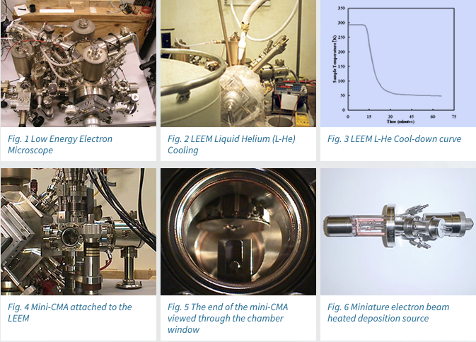
Low energy electron microscopy (LEEM) (Fig. 1) utilizes low energy, elastically backscattered electrons to image surfaces with high spatial and temporal resolution. Advantages of LEEM over other surface imaging techniques are:
- Real-time imaging capability
- Several unique contrast mechanisms for image formation
- Operation under extreme conditions
LEEM has been applied to a variety of problems including surface structure and morphology determination, dynamic processes (e.g., epitaxial growth, desorption, island decay, oxidation), surface and thin film magnetism. The LEEM at HKUST is one of only about a dozen in the world. LEEM is described in further detail at http://physics.ust.hk/department/phaltman/leem/

Special Features of LEEM at HKUST
The LEEM at HKUST boasts several unique/special features that were developed at HKUST.
- Liquid helium low temperature sample stage
We have developed the most advanced sample cooling stage available for the low energy electron microscope (LEEM) (Fig. 2). This apparatus cools samples very quickly to very low temperatures using liquid helium, isolates the microscope high voltage (-20kV), causes no sample vibrations during imaging, and allows sample transfer in vacuum. The sample cooling stage routinely achieves a sample temperature of 50K after a cooldown time on the order of only twenty minutes (Fig. 3).
- Miniature cylindrical mirror analyzer
[K.Grzelakowski, K.L. Man, and M.S. Altman, Rev. Sci. Instrum. 72, 3361 (2001)]
The mini-CMA comprises outer and inner cylinders, integral on-axis electron gun, and detector system, all mounted on a single 2.75" flange. Entrance angle, sample-to-detector distance, and polar cone angle were chosen, in consideration of second order focussing effects, that optimized analyzer transparency and resolution. Fringe field correction at the ends of the CMA is made by means of six rings precisely separated by sapphire insulators. The energy range of analyzed electrons can be varied between 0 eV to 3.0 keV. The flange mounting also incorporates a high precision z-motion drive for optimization of the working distance. The control electronics and software permit operation of the instrument in pulse and analog phase sensitive detection modes. Results obtained with this new mini-CMA demonstrate an energy resolution (Delta-E/E) of 0.9%, which is comparable to larger 6" flange-mounted instruments. The very small size of the mini-CMA permits its use in small or crowded ultra high vacuum chambers or where only 2.75" ports are available, thereby increasing flexibility in surface analysis. The images show one possible mounting configuration on the LEEM (Fig. 4),and a view of the end of the CMA through a chamber window (Fig. 5)
- Low noise, high resolution ccd camera with special data acquisition softwar
The LEEM at HKUST is equipped with a high resolution (1376 x 1040 pixels), high dynamic range (12-bit), low noise (2 stage peltier cooler with forced air), high frame rate (up to 10 frames per second at full resolution) ccd camera. The camera is the Sensicam QE version from PCO Computer Optics GmbH (www.pco.de). A dedicated software suite has been written at HKUST to support camera control, automated image acquisition and storage, including capabilities for spin polarized LEEM data acquisition and LEED spot profile measurements and analysis.
- Miniature electron beam heated deposition source
These deposition sources are mounted on a 2.75" flange, fit into tight space on the LEEM, and include water cooling, integral shutter and flux monitor by proportional ion current measurement. Material may be evaporated from rod or crucible. Materials that have been evaporated so far include Ag, Cu, Pd, Sb, In, Cr, Fe, Co, Pt.
- Sample holder with applied magnetic field capability